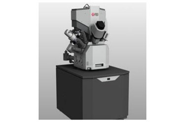
FEI Introduces Two New DualBeams For Materials Science

FEI on Thursday introduced two new DualBeam systems that feature innovative detection suites that provide high-quality imaging and fast analysis over the broadest range of samples. The new Scios DualBeam is specifically positioned for fast 2-D and 3-D characterization. The Helios NanoLab 660 DualBeam adds capabilities for specialized applications, such as the fabrication of prototypes for nanometer-scale devices.
“These new systems make it easier to image challenging materials,” said Trisha Rice, vice president and general manager of FEI’s Materials Science Business Unit. “Their new detectors are able to reveal the subtle details in surface contrast. The electron optics innovations in Scios make it especially powerful for investigation of challenging materials, like insulating or magnetic materials. The Helios NanoLab 660, with its advanced combination of patterning engine, MultiChem gas delivery system, and Tomahawk ion optics, provides unprecedented capabilities for fabricating prototypes of complex nanodevices, enabling researchers to pioneer developments in devices like antennas and nanofluidic systems.”
Rice added, “TEM usage is growing rapidly as researchers seek to understand structure-function relationships down to the atomic level. These new DualBeam instruments are designed to support efficient TEM workflows by producing samples that meet any TEM application requirement, from nanoscale analysis to atomic resolution imaging. This tight integration will become even more apparent in coming TEM product launches--stay tuned.”
For researchers working with materials that are difficult to image without coatings or preparation, the Scios offers technology innovations to mitigate these challenges. The new electron column is designed to handle characterization routines for both magnetic and non-magnetic samples. Its high-current capability provides fast x-ray analysis and can also be used to improve FIB milling accuracy on non-conductive samples by neutralizing accumulated charge.
The Scios also includes the new Trinity detector suite, comprising of three highly-efficient, in-lens detectors designed to detect electrons of different types and energies. Manipulating the detectors and mixing their signals allows the operator to selectively enhance material contrast, topographic contrast, edge detection, surface specificity and much more. This gives the user immediate access to a greater range of visual data from their sample for rapid characterization of materials.
The Helios NanoLab 660 DualBeam incorporates FEI’s second-generation extreme high-resolution scanning electron microscope (XHR SEM) technology, using proprietary electron optical and detector technologies to deliver sub-nanometer imaging resolution over the widest range of accelerating voltages (0.5-30 kV). This allows researchers working with delicate or beam-sensitive materials to have access to fine structural, nanoscale details without damaging their sample. Up to 100 nA SEM beam current enables fast analysis, and new in-lens detectors allow simultaneous topographic and materials contrast imaging, along with energy filtering. The Tomahawk FIB column guarantees the tightest beam at high and low currents, for fast, precise large-volume removal and polishing, respectively; and exceptional low-energy performance to remove surface damage, which is especially useful when preparing samples for atomic-scale TEM imaging.
NanoBuilder 2.0, a second-generation nanoprototyping toolset being introduced on the Helios NanoLab 660 DualBeam, simplifies and accelerates the fabrication workflow for nano- and micro-scale device prototypes. Starting with a CAD design, the NanoBuilder software directs FIB milling and deposition to build intricate 3D structures with features ranging in size from nanometers to millimeters.
These two new DualBeams join FEI’s Versa 3D system, configurable for dynamic experiments, to provide a portfolio of complementary FIB/SEM solutions for materials research applications.
Source: FEI
