CMOSIS Outlining Low Noise/High Dynamic Image Sensor Concept

At Vision 2010, CMOSIS was introducing a newly developed image sensor concept that yields very low dark noise and uses dual gain readout to increase the dynamic range above 89,5 dB. CMOSIS has shown a 1-Megapixel sample imager to demonstrate the pixel concept's superior performance. The new approach offers substantial advantages for numerous image processing tasks in scientific, diagnostic and security applications
The new CMOSIS image sensor concept is based on a special pixel type which dynamic range is increased by two distinct techniques. Most significant is its very low dark noise of less than 3.4 e- at a full well capacity of 100 ke-. Equally important is that the integration of the image charge takes place simultaneously at a low and a high amplification setting. The dual gain readout results in two different images. They are read out sequentially and combined externally into one final image, which dynamic range extends to more than 89,5 dB.
The image capture array based on this pixel type offers an electronic rolling shutter, whose lines can be selected and read out via the columns. Due to the twofold readout of each pixel, the sensor has twice the number of column amplifiers than columns. Their amplification factors are programmable at 1X to 16X. This yields a broad range of optical sensitivity.
Several multiplexers are provided to select the proper column and transfer the analog signals to a three-stage output circuit, which consists of an amplifier for correlated double sampling at 1X, 2X or 4X and programmable offset, limiter and output driver. This explains the exceptional flexibility of the new concept: analog/digital conversion can be done off-chip while programmable amplification and offset can adapt the sensor IC to different A/D converters. The limiter will spring into action when a subsequent converter needs more time to recover after a heavy overdrive – which is not tolerated by many applications.
Since the basic circuitry of this image sensor provides no on-chip runtime control, the pixel array is completely controlled externally. It comes with a serial interface that allows the setting of several internal registers for parameter selection.
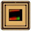
A demonstrator of the concept, first-time shown at Vision 2010, is the CLN1000 (CMOSIS Low Noise 1000K Pixel). The sample unit features a 1-megapixel array (1024 x 1024) laid out as a 10x10µm grid. Two amplifier paths (a total of 2048) per pixel column (total of 1024) minimize readout noise. Four analog output channels of 16 MSPS each, which can be combined via a 4:1 multiplexer to a 64 MSPS output, are driven by four 512:1 multiplexers and output stages. Maximum frame rate of this configuration is 20 fps. The CMOSIS CLN1000 sample is housed in a JLCC-84. It consumes about 300 to 350 mW of power.
Based on this 1-Megapixel sample unit, CMOSIS will design and implement a number of future sensor products for specific applications. These new products may integrate runtime control and on-chip analog/digital conversion and deliver higher frame rates and/or special pixel sizes. Among the manifold uses of the new CMOSIS dual gain readout sensor concept are scene monitoring and analysis, medical diagnostics, astronomy, microscopy and spectroscopy, industrial image processing, X-ray radiography, as well as luminescence- and fluorescence-based applications.
About CMOSIS
CMOSIS was established in 2007 and is a pure-play supplier of standard off-the-shelf and application-specific CMOS image sensors for the industrial and professional market covering applications such as machine vision, scientific, medical, automatic data capture and space. The company was conceived as a fabless CMOS image sensor vendor providing in-house design, characterization and qualification facilities for research, development and volume production. CMOSIS is growing consistently and currently employs about 30 people. CMOSIS is headquartered in Antwerp, Belgium.
SOURCE: CMOSIS
