Indium phosphide enables highly integrated fiber optic components

By Mee Koy Chin, Director of Technology Development
Nanovation Technologies, Inc.
Future telecommunications applications will need smaller, faster and more cost-effective optical components to meet the bandwidth demand. One way to meet this demand is through the integration of active and passive photonic components on indium phosphide (InP), in a way that mirrors the development of integrated electronics on Silicon that fueled the computer revolution.
As telecom equipment providers now scramble to meet the new demands for capacity, many are faced with the task of assembling systems from discrete optical components. Some of these components, such as demultiplexers, switches, and splitters, are already implemented in integrated optics. However, in most systems these piece parts are still housed in separate boxes, ganged together by loops of optical fiber. The high part counts, assembly costs, and fiber management headaches are already steering system developers toward larger scale integration, which offers an economic advantage.
Currently component integration is dictated by device groupings as determined by compatible materials systems. InP-based electronics, lasers, optical amplifiers, and electro-optic switches and modulators for the 1300-1600 nm fiber optic window have established a presence for InP in the telecommunications marketplace, but they are available only as discrete active components. For the moment, integration is limited to passive devices on common materials.
The integration of active and passive devices on InP will result in ultra-small, future-proof high-speed switching systems that open new doors in product line customization. Once these integrated circuits are perfected, they will replace discrete components because they will offer increased reliability and functionality while reducing size and cost and simplifying packaging. The additional advantages of integrated devices are improved signal-to-noise ratio, lower power consumption and reduced sensitivity to off-chip parasitics.
Why indium phosphide?
Component manufacturers for the photonic industry are aggressively developing ways to consolidate large numbers of separate devices into a single chip, customizing them for different applications, drastically reducing costs and improving performance.
A wide variety of materials, ranging from silica, silicon, and polymers to III-V compounds such as InP, are being used for different applications. Each one has its own advantages and drawbacks, both in terms of the performance of the resulting chip and in the ease and in the cost of manufacturing it. So far, the resulting integrated devices are relatively simple, standardized components such as DWDM chips, small switch modules, and passive splitters.
InP applications for discrete active devices are widespread in communications networking, making it the natural starting place for wholesale integration of passive devices for a complete system on a chip. As a semiconductor material, InP can provide all-in-one integrated functionality that includes light generation, detection, amplification, high-speed modulation and switching, as well as passive splitting, combining and routing. The same material can be used to make high-speed modulators, switches, amplifiers and detectors, or just passive waveguides for interconnecting these diverse devices.
Passive and active integration
In theory, the advantages of integrated optics were always clear. Ultra thin layers that could confine light, route it, and manipulate its properties would be far more compact and lightweight than bulk lenses and mirrors. Mass production techniques and large-scale integration would drive down the costs. Highly functional products, even full systems-on-a chip, would be easy to synthesize by integration of optical components.
Using strongly confined waveguides, active and passive devices can be built and integrated on InP. Through the small, tight waveguide design, passive devices can be made much more minute than previous versions, enabling a greater number of devices to be integrated on the same substrate.
Designing in indium phosphide
The general design of the waveguide can be considered in two dimensions. Vertically, the layers are identical to those of conventional waveguides with core and cladding layers. Nanovation's typical core layer is half a micron thick. The waveguides are etched deeply so that horizontally they are surrounded by air or another low-index medium such as polymer or oxide.
Due to the large difference in refractive index between the waveguide core material and the external medium, the light is strongly confined inside the waveguide. Such a large index difference only exists in semiconductors. Waveguides fabricated from other materials, such as silica and lithium niobate, are not strongly confined. The difference manifests itself in the radius with which the waveguides can be bent. For semiconductor waveguides, such a radius can be as small as a few microns, in contrast to millimeters or centimeters for silica or lithium niobate waveguides.
Thus, in InP designs, interconnections are much shorter because the waveguides can be routed with very small bending radii, allowing more devices to be to integrated together. Integration of active devices on the same chip is achieved using an integration platform that does not involve sophisticated material regrowth technology. By using one-step epitaxial growth and photolithographic processing, the integrated chip can be economically mass-produced.
Drawbacks of InP
Despite all of the advantages, InP is not without its limitations. One potential disadvantage with InP integration is that insertion loss tends to be high. Waveguides are much smaller compared to single-mode fibers, thus the coupling efficiency between the fiber and the waveguide is low. However, this is not a fundamental roadblock. Researchers are developing an approach that will lead to a fiber-to-waveguide coupling loss of 3 dB or less, which is sufficiently low for most photonic networking applications, particularly in highly integrated circuits.
Polarization-dependent loss is another potential disadvantage. In general, the strongly confined InP ridge waveguides are polarization sensitive. The coupling loss into these waveguide also can be a source of polarization dependence as well as some physical mechanisms used in the switching devices. Occasionally, positioning one polarization dependence against another can reduce the overall polarization dependence. The detailed optimal solution will depend on the intended applications.
InP devices
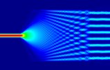
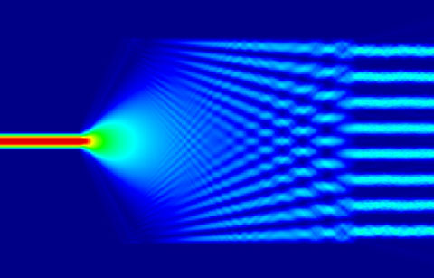
To design InP devices and optical circuits, we simulate performance using numerical mode solvers, beam propagation method and a finite difference time domain solutions. The simulation results can be verified through rapid prototyping via electron-beam direct-write pattern generation on wafers and a whole slew of device processing techniques. The resulting devices are then tested and the data fed back to the next design cycle in an iterative manner. Using the experimental and theoretical databases to generate abstract models for the underlying devices, Nanovation is developing a photonic CAD software tool for circuit-level design that customers can use to develop custom-designed integrated circuits (see Figure 1).

Even when the integration of active and passive devices on InP becomes possible, it must become affordable before it will be readily accepted within the telecommunications industry. Systems integrators are looking to their component suppliers for low cost solutions, rapid time to market, and innovative features that will set them apart from other equipment suppliers. The vendors that offer integrated photonic circuits based on InP can provide early adopters a custom, low-cost chip with their choice of lasers, optical amplifiers, switches, and photo detectors for the 1500-1600 nm fiber optic window as well as passive optical circuit elements such as demultiplexers, splitters, couplers, and taps.
About the author
Dr. Mee Koy Chin is director of technology development at Nanovation Technologies. He joined Nanovation in 1998 to establish and operate the company's clean room fabrication laboratory at Northwestern University. Dr. Chin coordinates the various phases of product development for Nanovation, from conceptual design to testing and packaging.
Nanovation Technologies, Inc.
1801, Maple Avenue,
Evanston, IL 60201
Tel: (847) 4675647
Email: mkchin@nanovation.com
