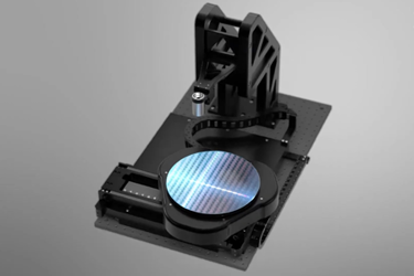
Semiconductor Wafer Inspection And Metrology With Multi-Axis Air Bearing Stage

Ensuring the quality and reliability of semiconductor chips demands meticulous precision at every stage of manufacturing. As technology advances and components shrink, the need for robust inspection tools capable of detecting defects down to the nanometer range becomes paramount. PI, a leader in precision motion control, offers an integrated solution tailored to the exacting demands of chip manufacturing.
This application note delves into the key features of PI's Air Bearing and Focusing Multi-Axis Motion Solution, highlighting its high speed, accuracy, and adaptability for surface inspection. From laser focus control to tip/tilt wafer alignment stages and low-profile XY scanning, discover how PI's engineered solutions optimize efficiency, reliability, and yield in semiconductor production.
Get unlimited access to:
Enter your credentials below to log in. Not yet a member of Photonics Online? Subscribe today.
